(Hong Kong)

Product Summary
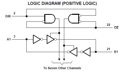
The SN74LVC8T245DGVR is a 8-bit dual-supply bus transceiver with configurable voltage translation and 3-state outputs. This 8-bit noninverting bus transceiver uses two separate configurable power-supply rails. The SN74LVC8T245DGVR is optimized to operate with VCCA and VCCB set at 1.65 V to 5.5 V. The A port is designed to track VCCA. VCCA accepts any supply voltage from 1.65 V to 5.5 V. The B port is designed to track VCCB. VCCB accepts any supply voltage from 1.65 V to 5.5 V. This allows for universal low-voltage bidirectional translation between any of the 1.8-V, 2.5-V, 3.3-V, and 5.5-V voltage nodes. The SN74LVC8T245DGVR is designed for asynchronous communication between two data buses. The logic levels of the direction-control (DIR) input and the output-enable (OE) input activate either the B-port outputs or the A-port outputs or place both output ports into the high-impedance mode. The device transmits data from the A bus to the B bus when the B-port outputs are activated, and from the B bus to the A bus when the A-port outputs are activated. The input circuitry on both A and B ports is always active and must have a logic HIGH or LOW level applied to prevent excess ICC and ICCZ.
Parametrics
Absolute maximum ratings: (1)Supply voltage range, Vcca,Vccb: -0.5 to 6.5V ; (2)Input voltage range, VI, I/O ports (A port) -0.5 to 6.5V; (3)Input voltage range, VI, I/O ports(B port): -0.5 to 6.5V; (4)Input voltage range, VI, Control inputs: –0.5 to 6.5V; (5)Voltage range applied to any output in the high-impedance or power-off state, A port, VO: –0.5 to 6.5V; (6)Voltage range applied to any output in the high-impedance or power-off state, B port, VO: –0.5 to 6.5V; (7)Voltage range applied to any output in the high or low state, A port, VO: –0.5 to VCCA+0.5; (8)Voltage range applied to any output in the high or low state, B port, VO: –0.5 to VCCB+0.5; (9)Input clamp current, VI<0, IIK: -50mA; (10)Output clamp current, VO<0, IOK: -50mA; (11)Continuous output current, IO: ±50mA; (12)Continuous current through each VCCA, VCCB, and GND: ±100mA; (13)Package thermal impedance, DB package, qJA: 63℃/W; (14)Package thermal impedance, DBQ package, qJA: 61℃/W; (15)Package thermal impedance, DGV package, qJA: 86℃/W; (16)Package thermal impedance, PW package, qJA: 88℃/W; (17)Package thermal impedance, RHL package, qJA: 43℃/W; (18)Storage temperature range, Tstg: -65 to 150℃.
Features
Features: (1)Control Inputs VIH/VIL Levels Are Referenced to VCCA Voltage; (2)Latch-Up Performance Exceeds 100 mA Per JESD 78, Class II; (3)VCC Isolation Feature, If Either VCC Input Is at GND, All Are in the High-Impedance State ; (4)ESD Protection Exceeds JESD 22; (5)4000-V Human-Body Model (A114-A); (6)200-V Machine Model (A115-A); (7)1000-V Charged-Device Model (C101); (8)Fully Configurable Dual-Rail Design Allows Each Port to Operate Over the Full 1.65V to 5.5V Power-Supply Range.
Diagrams
| Image | Part No | Mfg | Description |  |
Pricing (USD) |
Quantity | ||||||||||||
|---|---|---|---|---|---|---|---|---|---|---|---|---|---|---|---|---|---|---|
 |
 SN74LVC8T245DGVR |
Texas Instruments |
Translation - Voltage Levels 8-Bit Dual-Supply Bus Xcvr |
Data Sheet |
|
|
||||||||||||
|
SN74LVC8T245DGVRG4 |
Texas Instruments |
Translation - Voltage Levels 8B Dual Supply Bus Transceiver |
Data Sheet |
|
|
||||||||||||